
MMIC technology

Figure 1: GaAs-MeSFET power amplifier module in MMIC technology
MMIC technology
MMIC (Monolithic Microwave Integrated Circuit) technology is a technology for manufacturing active and passive components on a monocrystalline substrate. These circuits can then be operated up to a relatively high cut-off frequency.
GaAs MeSFETs are often used in solid-state high-power amplifiers for radar sets.
| Technology | use area | remarks |
|---|---|---|
| Silicium- bipolar and CMOS | <6 GHz | BJT: high amplifications, small tolerances, Silicium substratum: dielectric with high losses. Very high mask costs for custom-designed MMICs. Suitable for mixedly analog/digital wirings. |
| Silicium-Germanium- bipolar (Si-Ge) | <10 GHz | Very complex and expensive process. Suitable for mixedly analog/digital wirings. |
| GaAs-MESFET | <10 GHz | Simple technology: economical for custom-designed wirings with small quantities. Suitable for high power amplifiers. |
| GaAs-hetero-bipolar transistors (HBT) | <20 GHz | Suitable for fastest digital circuits, oscillators and power amplifiers. |
| Indium-phosphid- HEMT (InP) | <100 GHz | InP-HEMT: best microwave qualities for small signals and low noise. |
| Indium-phosphid-HBT (InP) | <230 GHz | Suitable for fastest digital circuits. |
| Gallium nitride HEMT (GaN) | <400 GHz | Used in transmit/receive modules of active antennas; best power and noise characteristics with smaller space requirements. |
Table 1: Overview MMIC- Technologies
Typically, discrete semiconductor devices, such as power transistors, cannot be connected in parallel without issues. Minor differences in their conductivity could cause one transistor to dominate, heat up more, conduct better, and eventually fail. However, if these transistors are manufactured with high precision on the same monolithic substrate, all transistors have consistent properties. This allows for parallel connections to be feasible.

p-material
n-material
Figure 2: Band model of a tunnel diode.

p-material
n-material
Figure 2: Band model of a tunnel diode.
Gallium arsenide (GaAs)
Gallium arsenide (GaAs) is a binary compound of the elements gallium and arsenic and is therefore an important Ⅲ-Ⅴ semiconductor material. A Ⅲ-Ⅴ semiconductor is defined as a compound semiconductor consisting of an element from group Ⅲ (e.g., boron, aluminum, gallium, indium) and an element from group Ⅴ (e.g., nitrogen, phosphorus, arsenic, antimony) of the periodic table. Due to their larger energy band gap (see Figure 2), GaAs devices are relatively insensitive to overheating and, especially at high frequencies, also tend to generate less noise in electronic circuits than silicon devices.
With its high power and wide frequency range, gallium arsenide is used in integrated MMIC circuits for power amplifiers in transmitter/receiver modules in active antennas or as amplifier modules in transmitters with passive antennas. Mass production has reduced the initially very high price, so that these circuits can also be used in the mobile communication.

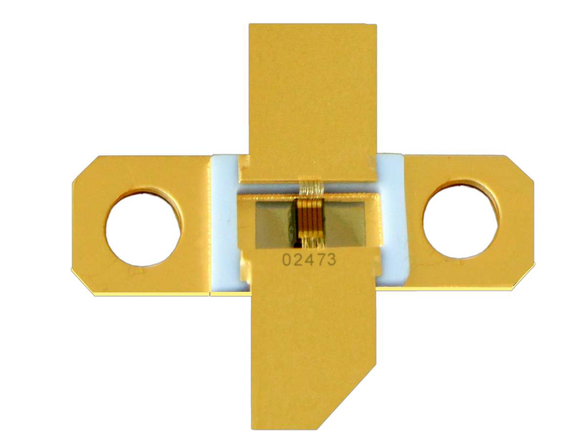
Figure 3: High-power MESFET in MMIC technology with cover removed
Gallium nitride (GaN)
Gallium nitride (GaN) is a binary compound of gallium and nitrogen. It is also a Ⅲ-Ⅴ semiconductor with a wide band gap, enabling higher power density and better efficiency than traditional silicon MOSFETs and bipolar transistors. GaN conducts electricity more efficiently than pure silicon, reduces power loss, and minimizes the need for cooling components. It allows for smaller, lighter systems by packing more power into a smaller space.
Particularly high efficiency in solar systems is achieved by manufacturing solar modules with GaAs technology and using GaN-based circuits in power converters.